Opto-electronic and all-optical devices:
One major emphasis of the research has been the investigation of optoelectronic devices that are compatible with the CMOS technology. We have proposed and designed a novel optical device, referred to as Surface Plasmon Polariton Diode (SPPD), where Surface Plasmon Polaritons (SPPs) are excited and then propagate along the interface of highly n-doped semiconductor substrate and lightly p-doped adjacent layer. We have developed highly efficient numerical and analytical methods to study and assess the SPPD switching characteristics for different applied bias voltages, doping concentrations of both p- and n-layers, as well as the thickness of the p-layer and the width of the active drift region. The developed numerical code self-consistently couples and solves the complex Multiphysics involved in the operation of the SPPD. The proposed SPPD operates at a transmission modulation higher than 90% (an order of magnitude higher compared to the current best performers). Using the SPPD as an impute waveguide, we have shown the possible all four SPPD logic gates (AND, NAND, OR and NOR).
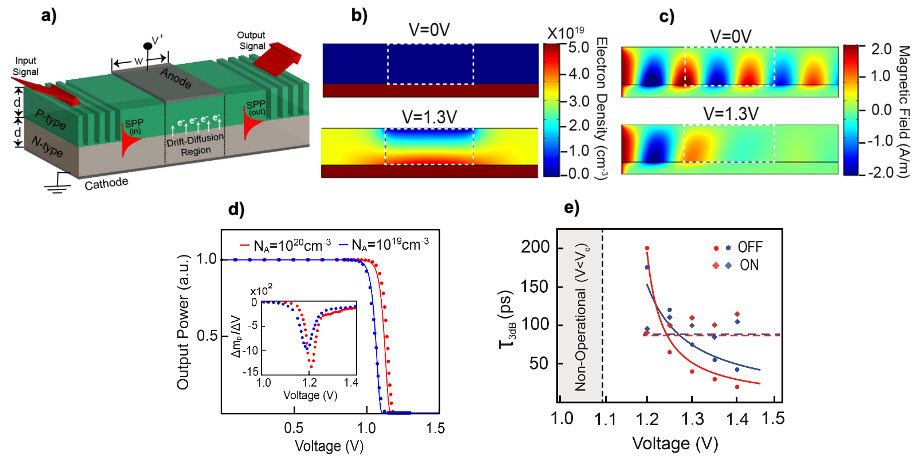
Fig.1. Silicon SPPD (a) Basic schematic of a Surface Plasmon Polarition Diode (SPPD). (b) Steady state minority carrier concentration profiles at different applied voltages. (c) Surface Plasmon Polariton (SPP) propagation along the length of the device. (d) The SPPD transmittance for Si with different P-doping concentrations are obtained using the self-consistent Multiphysics model (dots) and compared to the WKB approximation (solid lines). The corresponding responsivities are shown as inserts. (e) Dependence of the SPPD OFF and ON times on the applied voltage (V>V
c). The device OFF time is dependent on the electron drift into the p-region and is thus inversely proportional to the applied voltage. In the calculations the operation frequency is set at 30THz, the thickness of the P-type layer is d=1.5μm, n
b identifies the refractive index of P- layer and the overall length of the active drift-diffusion region is fixed at w=4μm.
EM properties of particle arrays and optical elements:
Selective laser melting (SLM) is an advanced rapid prototyping technique that is capable to manufacture components with no geometric constraints. The fabrication process is complex and it’s necessary to develop a complete theoretical model of the coupled electromagnetic and thermodynamic processes involved in the SLM. During the past research efforts, we have developed analytical and numerical model and performed full theoretical investigation in order to better understand the Multiphysics involved in SLM. Our studies show that excitation of SP states in the gaps of metal powders concentrate large amounts of EM energy in very small spatial areas resulting in improved energy absorption and fast microsecond thermalization. Near-unity absorption mechanism can be obtained for periodic particles with sizes that support first order cavity resonances. We have acquired extensive numerical data representing the local laser heating and temperature profiles for steady-state and transient illumination. The numerical results were compared with analytically calculations showing an excellent agreement. The analytical model is also shown to provide a qualitative and quantitative description of the volumetric temperature rise in the powder beds as a function of optical and thermometric parameters. Selective control of the particle shape and size could be used to achieve high order of control over the coupling between the incident EM fields and the SP modes, further helps to reveal the optimal parametric space related to applied laser power, scan velocity, powder material, layer thickness and porosity.
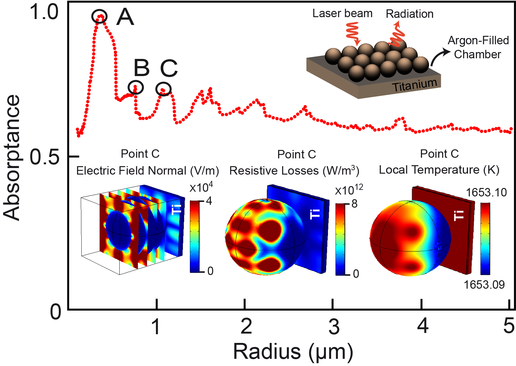
Fig.2. Absorptance versus particle size for closely packed (touching) titanium spheres arranged in square lattice on top of a titanium substrate (see insert). Also, the corresponding the local electric field, resistive losses and local temperature for point C is shown in the insert. In the calculations the laser radiation is normal to the particle bed and the laser wavelength is set at 1.070μm and P
0=40W/cm
2.